Thin-Film Lithium Niobate Foundry Services by CSEM
Powered by CSEM, delivered by CCRAFT
CSEM is the pioneer of industrial-grade TFLN PIC technology with a robust PDK and 150 mm wafer process. New: Customer-facing TFLN-PIC foundry services are now operated via CSEM spin-off CCRAFT, ensuring global scalability.
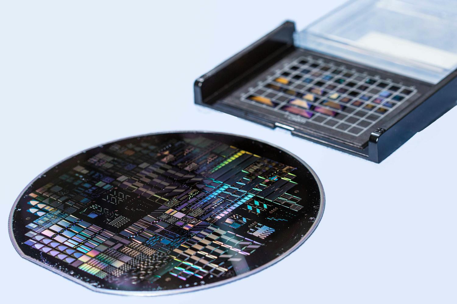
CSEM is the pioneer of industrial-grade Thin-Film Lithium Niobate (TFLN) photonic integrated circuit (PIC) technology, supported by a robust process design kit (PDK) and a 150 mm wafer-scale workflow for design, manufacturing, and testing.
To accelerate global adoption, customer-facing TFLN PIC foundry services — including design, wafer processing, PDK access, prototyping, and volume production — are now operated by CCRAFT, a CSEM spin-off created to scale this breakthrough technology while leveraging CSEM’s processes and know-how.
CSEM continues to drive photonics innovation through research collaborations, system demonstrators, and advanced development services across optical and microtechnology platforms beyond TFLN. For photonics R&D, integration expertise, or collaborative innovation, our team remains ready to engage.
Learn how Miraex leveraged our TFLN foundry services for breakthrough photonics solutions.
Looking for the next MPW run?
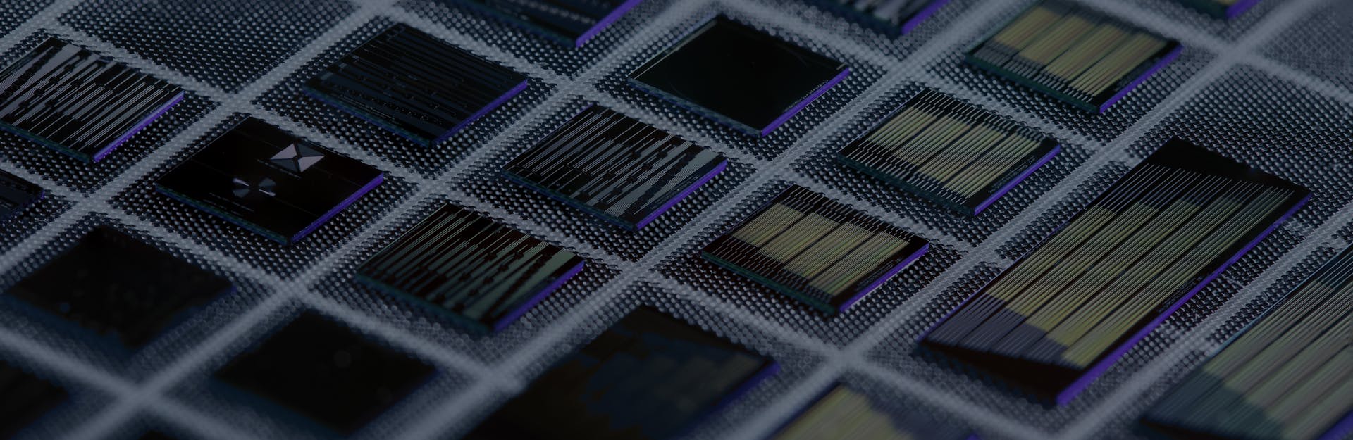
TFLN PIC manufacturing is now handled by our spin-off company CCRAFT, which continues the service with enhanced capabilities and regular Multi-Project Wafer (MPW) schedules.
CSEM’s ongoing technology and R&D role
While CCRAFT manages operational foundry services, we continue to advance the integrated photonic platforms with process innovation, device integration, and application-specific development. We collaborate with industry and academia to push photonic performance limits and explore novel architectures for telecom, quantum, datacom, and sensing applications.
CSEM focuses on:
- Advancing the integrated photonic and MEMS platforms through process innovation and integration of novel devices.
- Developing next-generation photonic components for telecom, datacom, quantum, and sensing applications.
- Building system demonstrators to validate new architectures and enable rapid adoption.
- Collaborating with academia and industry to explore novel applications.
- Providing integration support for hybrid and heterogeneous photonic systems.
Check out our flagship EU projects!
Meet our happy customers
Mikkel Heuck
Research Scientist Quantum Photonics Laboratory
We are strong supporters of CSEM’s efforts to build up a foundry service for lithium niobate integrated photonics since we believe it will have a major impact on both industry and the scientific community. It is really a fortunate situation for us to get in early and work with CSEM as their capabilities expand and accelerate our research in integrated quantum photonics.
MIT

Richard Phelan
Head of laser design
We’ve had several projects with CSEM, which have advanced our semiconductor laser products substantially and opened up new commercial opportunities in the area of low linewidth lasers for lidar applications. The discussions with the experts at CSEM have provided us with many new ideas as well as valuable feedback for different applications such as metrology and sensing.
Eblana Photonics
Augustinas Vizbaras
CTO
CSEM has a fantastic understanding and knowledge of using optical systems to measure vital signs, and bringing this know-how into our use case has allowed us to make huge improvements in our OptiBP software—and potentially in the global management of hypertension.