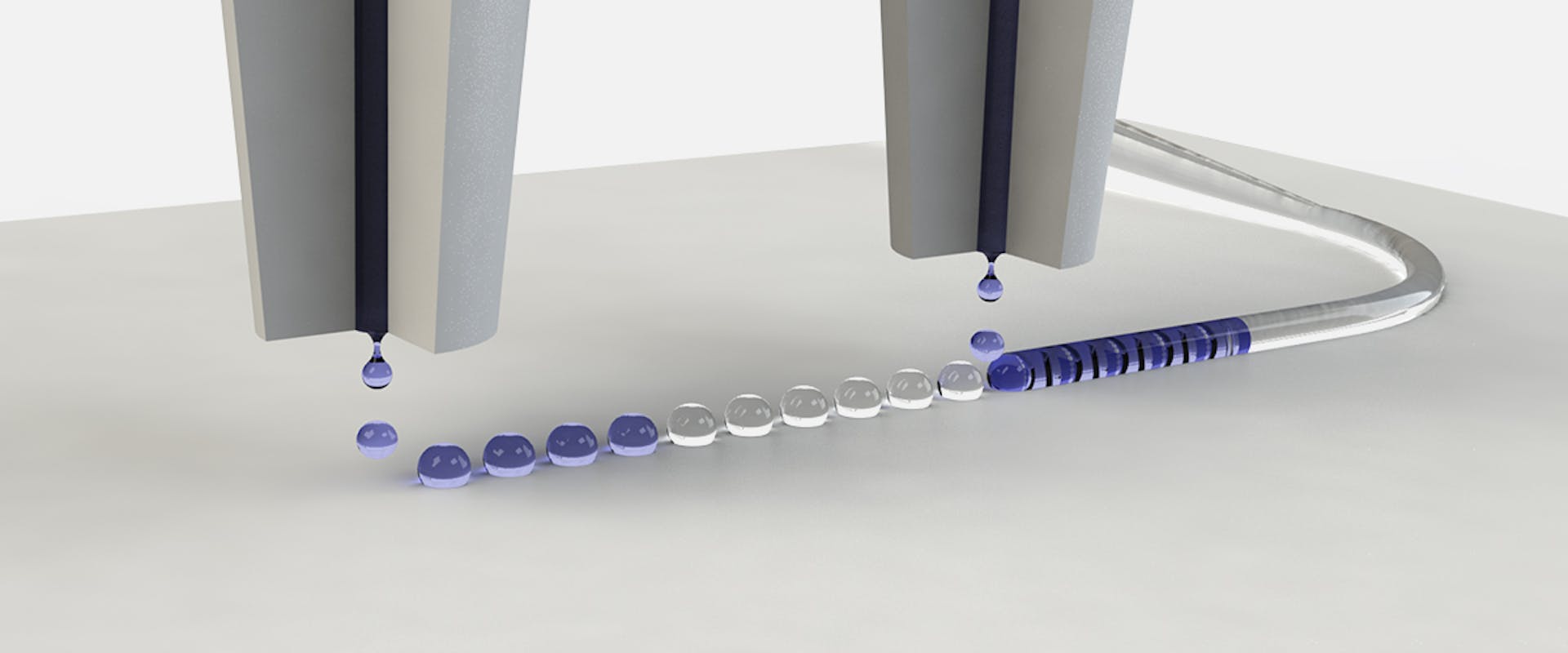
Micro optical components such as optical waveguides have proved very difficult to create with inkjet printing. The surface tension of the inks makes it difficult to print the smooth shapes and lines of a specific height vital for such elements. CSEM's researchers discovered that depositing the ink in two steps rather than one can overcome both these problems.
CSEM's technique outperforms existing options in a number of ways. As a highly customizable additive manufacturing method, it enables a high degree of freedom in testing ideas and concepts for new devices by varying design parameters. It also allows a great deal of flexibility in connecting optical components.
"The fact that our approach could allow components with multiple functionalities to be fabricated with a single printer paves the way toward additive manufacturing of entire integrated circuits on chips," says CSEM's researcher Fabian Lütolf. "This means that passive optical components could be combined with active flexible hybrid electronics devices, for example printed lighting devices such as printed LEDs or printed sensors."
CSEM is now working to demonstrate the applicability of the printed micro optical devices to real-world applications in order to enable the technology's transfer to industry.
Useful links