Thin-Film Lithium Niobate Foundry Services by CSEM
Powered by CSEM, delivered by CCRAFT
CSEM is the pioneer of industrial-grade TFLN PIC technology with a robust PDK and 150 mm wafer process. New: Customer-facing TFLN-PIC foundry services are now operated via CSEM spin-off CCRAFT, ensuring global scalability.
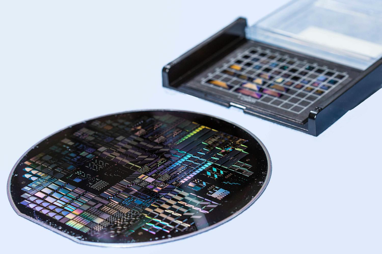
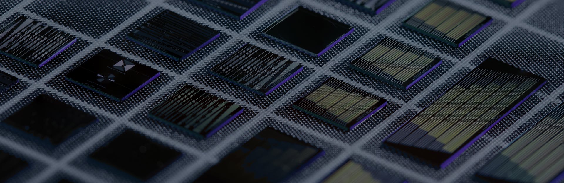
CSEM is the pioneer of industrial-grade Thin-Film Lithium Niobate (TFLN) photonic integrated circuit (PIC) technology, supported by a robust process design kit (PDK) and a 150 mm wafer-scale workflow for design, manufacturing, and testing.
To accelerate global adoption, customer-facing TFLN PIC foundry services — including design, wafer processing, PDK access, prototyping, and volume production — are now operated by CCRAFT, a CSEM spin-off created to scale this breakthrough technology while leveraging CSEM’s processes and know-how.
CSEM continues to drive photonics innovation through research collaborations, system demonstrators, and advanced development services across optical and microtechnology platforms beyond TFLN. For photonics R&D, integration expertise, or collaborative innovation, our team remains ready to engage.
Learn how Miraex leveraged our TFLN foundry services for breakthrough photonics solutions.
Looking for the next MPW run?
TFLN PIC manufacturing is now handled by our spin-off company CCRAFT, which continues the service with enhanced capabilities and regular Multi-Project Wafer (MPW) schedules.
CSEM’s ongoing technology and R&D role
While CCRAFT manages operational foundry services, we continue to advance the integrated photonic platforms with process innovation, device integration, and application-specific development. We collaborate with industry and academia to push photonic performance limits and explore novel architectures for telecom, quantum, datacom, and sensing applications.
CSEM focuses on:
- Advancing the integrated photonic and MEMS platforms through process innovation and integration of novel devices.
- Developing next-generation photonic components for telecom, datacom, quantum, and sensing applications.
- Building system demonstrators to validate new architectures and enable rapid adoption.
- Collaborating with academia and industry to explore novel applications.
- Providing integration support for hybrid and heterogeneous photonic systems.
Check out our flagship EU projects!
Meet our happy customers
Mikkel Heuck
Chercheur scientifique laboratoire de photonique quantique
Nous soutenons fortement la démarche du CSEM visant à construire un service de fonderie pour cristaux photoniques en niobate de lithium, car nous croyons que cela aura un impact majeur sur l’industrie et sur la communauté scientifique. Nous avons une chance incroyable d’avoir été associés très tôt à cette démarche et de travailler avec le CSEM, dans la mesure où ses capacités étendent et accélèrent notre recherche dans le domaine de la photonique quantique intégrée.
MIT

Richard Phelan
Responsable conception laser
Plusieurs projets réalisés avec le CSEM nous ont permis d’effectuer des avancées substantielles dans les lasers à semi-conducteurs et nous ont ouvert de nouvelles opportunités commerciales dans les lasers à raie ultrafine pour les applications LIDAR. Les discussions avec les experts du CSEM nous ont apporté de nombreuses idées nouvelles et des retours utiles pour différentes applications telles que la métrologie et la détection.
Eblana Photonics
Augustinas Vizbaras
Directeur technique
Le CSEM possède une connaissance et une maîtrise incroyables des systèmes optiques permettant de mesurer les signes vitaux. Il a utilisé ce savoir-faire pour nous aider à atteindre notre objectif, nous permettant ainsi d’améliorer considérablement le logiciel OptiBP et, par conséquent, la gestion de l’hypertension à l’échelle mondiale.