Micro and nano optics

Extreme light control. Industrial-grade innovation

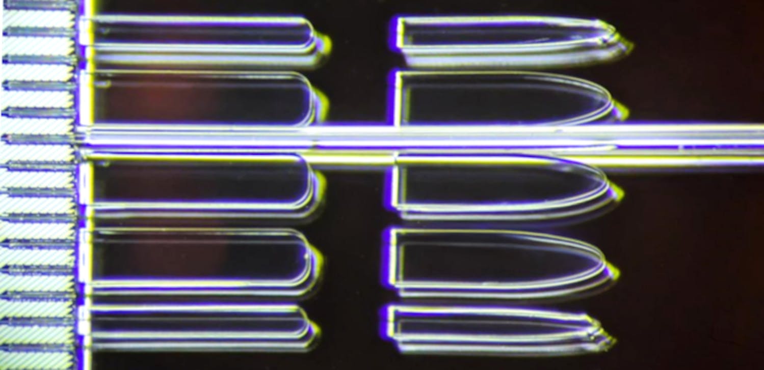
on-chip microlens arrays on packaged space-qualified CMOS imagers

CSEM specializes in the development and industrialization of advanced micro- and nano-optical components and subsystems, tailored to specific applications. Our expertise is built on over 40 years of delivering cutting-edge micro- and nanofabrication solutions.

These components are integrated across high-tech sectors: automotive, consumer electronics, life sciences, aerospace, communications, document security, brand protection, watchmaking, and more.

What we offer in micro-nano optics

We cover the full innovation chain, adhering to ISO 9001 standards. Whether you need a standalone service or end-to-end support, we adapt to your goals—from prototyping to pre-production.

Optical design & simulations

We use multiphysics simulation platforms to design and optimize optical structures. Capabilities include:

  • Ray tracing for imaging/illumination
  • Diffractive and guided mode optics
  • Light concentration on active complex imager chips and wafers
  • Subwavelength resonances and near-field effects

Micro- and nano-fabrication for prototyping and pilot series

Our cleanroom infrastructure supports full fabrication from master origination to pilot-scale replication:

Origination – we create high-precision master structures that define the optical function of the final component, using:

  • Microlens arrays by photoresist reflow
  •  Electron-beam lithography (EBL)
  • Complex mastering (two-photon grayscale lithography, diamond turning) with partners

These enable precise fabrication of microlens arrays, free-form optics, and diffractive structures. Masters are replicated via wafer-scale nanoimprint lithography or UV molding.

Replication and pilot production we fabricate on up to 8-inch wafers, using:

  • Photolithography
  • Nanoimprint lithography
  • UV molding
  • Hot embossing
  • Thin-film deposition

Larger surfaces are processed on our roll-to-plate nanoimprint device dedicated to pilot production..

Tooling for mass production

We manufacture tooling for industrial volumes:

  • Injection mold structuring
  • Nickel shim production
  • Step-and-repeat master upscaling
  • Steel-to-steel or steel-to-titanium marking

We also offer process consulting for scaling up from pilot to volume manufacturing.

Materials and optical structures

We work with a wide range of optical-grade materials to support the design, origination, and replication of micro- and nano-optical components. We use materials tailored for optical transparency, thermal/mechanical stability, and wafer-level compatibility.

Materials and substrates portfolio

  • Polymers: UV-curable resins, Ormocer®, PMMA, PDMS, COP/COC, PET, PC – ideal for nanoimprint lithography and UV molding
  • Metals: aluminum, nickel, titanium, steel – used for reflective optics, plasmonic structures, or tooling (e.g., nickel shims)
  • Dielectrics: silicon dioxide (SiO₂), silicon nitride (Si₃N₄), titanium dioxide (TiO₂), zinc sulfide (ZnS), magnesium fluoride (MgF₂) – for waveguides, filters, or multilayer stacks
  • Semiconductors: silicon and CMOS wafers (BEOL only), III-V wafers – for integration with photonic and electronic chips or meta-optics
  • Glass: borosilicate, fused silica, radiation-resistant glass – for high-precision optics and space-grade applications
  • Ceramics and thin foils – for high-temperature or harsh-environment applications.

Optical structures

  • Microlens arrays (MLAs) for beam shaping, light collection, and image sensor enhancement
  • Freeform microlens array / freeform micro-optics 
  • Diffractive gratings for beam expansion, spectral filtering, laser pulse compression, and waveguide coupling
  • Waveguides for integrated photonics and light routing 
  • Plasmonic and meta surfaces for color filtering, light steering, and security features
  • Subwavelength structures for anti-counterfeiting and high-efficiency holograms

Metrology and quality control

Our metrology services ensure that micro- and nano-optical components meet the highest standards of precision, reproducibility, and optical performance. These services are critical to both R&D validation and industrial quality control.

We offer nanometer-to-micrometer resolution metrology:

  • Scanning Electron Microscopy (SEM) – for high-resolution surface imaging
  • Atomic Force Microscopy (AFM) – for 3D surface profiling and nanostructure analysis
  • Laser confocal microscopy on very large substrates – for non-contact 3D imaging of micro-optical surfaces
  • Automated white-light Interferometry – for surface flatness and step-height measurements
  • Profilometry – for surface roughness and form factor evaluation
  • Wafer-scale automation – for high-throughput inspection of micro-optical arrays

 Metrology supports

  • Design validation 
  • Process control in wafer replication
  • Optical performance benchmarking 
  • Tool qualification for nanoimprint and injection molding masters

Optical testing

  • Spectral transmission, reflection, and scattering measurements
  • Wavefront error and focal length testing for microlenses
  • Diffractive efficiency and angular response of gratings
  • Alignment and coupling efficiency for photonic integrated circuits
microlens array

Start your optical innovation journey with us

From feasibility studies to scalable fabrication, CSEM helps you bring advanced micro- and nano-optical solutions to life. Let’s tackle your challenge—together.

Applications and use cases

Our micro- and nano-optical technologies power innovation across diverse sectors—from sensing and imaging to communications, security, and wearable displays. Below are examples of how our solutions translate into real-world applications, delivering performance, scalability, and integration at the wafer level.

Micro-optical arrays

Hexagonal array of nearly gapless MLA with 23 µm pitch.

Microlens arrays (MLAs) enhance sensor performance by maximizing photon capture per pixel. They also play a critical role on the emission side, where MLAs shape the output of sources such as VCSELs for efficient fiber coupling in transceiver modules, beam profiling in sensing applications, and structured illumination.

We provide end-to-end support, from design to fabrication, including specialized services like our microlens array foundry and technical lead participation in the Phabulous pilot line for free-form micro-optics.

Key benefits:

  • Enhanced light collection and beam control
  • Scalable, cost-efficient fabrication via UV molding and photolithography
  • Direct integration at chip or wafer level.

Fiber alignment and coupling on photonic integrated circuits

Passive fiber alignment and coupling onto silicon nitride photonic integrated circuits, realized by wafer-scale imprint of microstructures.

We realize passive fiber alignment, using micro-optical elements and integrated comb structures, fabricated through wafer-scale reflow and UV molding processes. Our approach combines light-redirection optics with self-alignment features to enable:

  • Efficient, low-loss coupling
  • High-precision fiber placement through passive alignment
  • Seamless integration into photonic integrated circuits at wafer scale

Key benefits:

  • Reduced insertion losses
  • Scalable manufacturing via photolithography and nanoimprint lithography
  • Cost-efficient assembly with facilitated fiber alignment for volume production

Diffractive waveguides for compact photonic systems

Diffractive light guide for beam expansion with a minimal footprint in a miniature atomic clock

We design and fabricate diffractive optical structures that couple light into integrated waveguides with exceptional efficiency and minimal footprint. These components are key enablers in biosensing, quantum optics, and miniature imaging systems such as AR/VR glasses and endoscopes.

Our approach combines nanoimprint lithography with thin-film deposition, enabling wafer-scale manufacturing of high-precision diffractive elements.

Applications include biosensing, quantum systems, or imaging (augmented reality, endoscopy). We realize our diffractive waveguides by using a combination of nanoimprint and thin film deposition.

Key benefits:

  • Efficient light coupling in ultra-compact photonic architectures
  • Scalable fabrication for mass production
  • Seamless integration with photonic chips, sensors, or optical stacks

Optical security for documents, devices, and consumer brands

Steel insert for injection molding structured with a hologram

We develop optical security features to protect official documents, luxury products, and industrial components from counterfeiting. These elements are based on micro- and nano-optical elements, including diffractive elements, subwavelength structures, and waveguides, making them visually distinctive and extremely difficult to replicate.

Our solutions are applied to a variety of substrates, including films and foils for packaging and labeling, steel inserts for injection molding, and functional surfaces for direct product integration.

We leverage four decades of experience in the field to support our clients with technology watch and consulting.

Key benefits:

  • Counterfeit-resistant, visually distinctive security features
  • Compatible with diverse materials, finishes, and colors
  • Industrial-grade fabrication using scalable, standardized processes

Beam shaping and waveguide coupling on PICs

SEM image and ray-tracing simulations for two wavelengths
Microlens on PIC C-band grating coupler (1490 and 1610 nm) for beam-shaping/fiber coupling.

We engineer micro-optical elements that are monolithically integrated into photonic integrated circuits (PICs) to perform advanced beam manipulation and coupling functions directly on the chip. Our approach enables:

  • Precise beam shaping of PIC emissions
  • Improved incoupling efficiency with relaxed alignment tolerances
  • Broadband, quasi-achromatic performance using refractive micro-optics—compatible with diffractive and meta-optical designs

Key benefits:

  • From custom optical design to chip-scale prototyping and wafer-level production (up to 200 mm)
  • Scalable processes compatible with wafer-level manufacturing processes and standard PIC substrates
  • Cost-efficient thanks to wafer-scale alignment and assembly integration

Explore what’s possible with micro- and nano-optics

Partner with us to co-develop your next breakthrough. Whether you're scaling up, solving a tough photonics challenge, or exploring disruptive applications, our experts are ready to support your innovation.

Related publications

Explore our publications below. Some articles may require a subscription or institutional access.